Layout Versus Schematic Verifcation
A successful DRC ensures that the layout passes through the rules designed
for faultless fabrication. However, it doesnot guarantee if it really
represents
the circuit you desire to fabricate. In our case for an inverter, we
really need
a tool which can compare our layout with the schematic and ensure that it is
really a layout for an inverter. One way Cadence does this is by generating a
spice netlist from the layout and comparing it with the spice netlist for the
schematic. This is the essence of the the LVS tool.
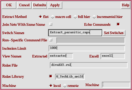
1. From the layout window, choose Extract... under the Verify menu. A window will pop-up. Make sure that the entries are as given below. For the entry in Switch Names, Click on Set Switches.. A window will pop-up. Choose the option for Extract_parasitic_caps. Finally click on OK.
- Make sure that your layout window is in Edit mode.
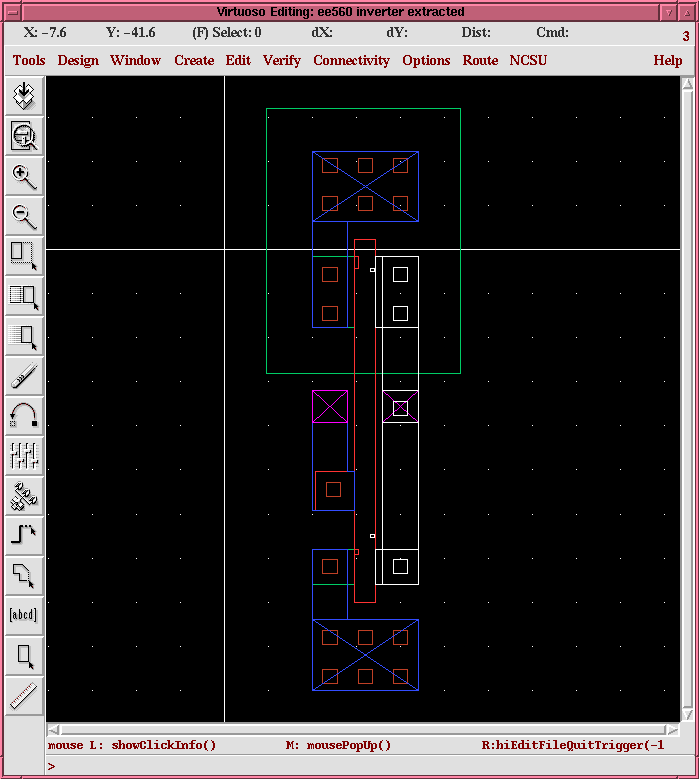
3a. Open the extracted view of the cell in edit mode. The extracted view will look something like this.
Just for fun, if you zoon in to those small (really small) rectangles in the poly area of the above figure, you will see either nmos4 and pmos4 written on it. This shows that the cadence has recognized that - that particular portion of the layout belongs to the transistors. Press Shift -F to see the symbols for the active and passive devices come up in the extract window. This is just symbolic to asscoaite the portions of the layout with different devices. It doesnot bear any connectivity information.
The next step is LVS. Since we generated a layout with certain W and L for
the transistors ( for the case discussed here, the author had nmos W =
8u and L
= 2.4u and pmos with W = 4u and L = 2.4u), the layout versus schematic
operation
(discusses below) will give you an error , if the schematic against which the
layout is compared has a different W and L for it's pmos and nmos transistors.
So make sure that nmos and the pmos has correct entries in their properties
field.
3 b. From the extracted window, choose LVS... under the Verify menu. A pop up menu will appear. Type in the run directory as well as the cell names that you want to run LVS on and all the other fields as shownin the inverter example below. It is advisable to put the run directory in the /tmp/username as you might run out of memory space when running huge layouts. If you already had an LVS directory, a window will pop-up which might say " The selected LVS rule directory does not match the run form". Just click on Form contents and click ok.
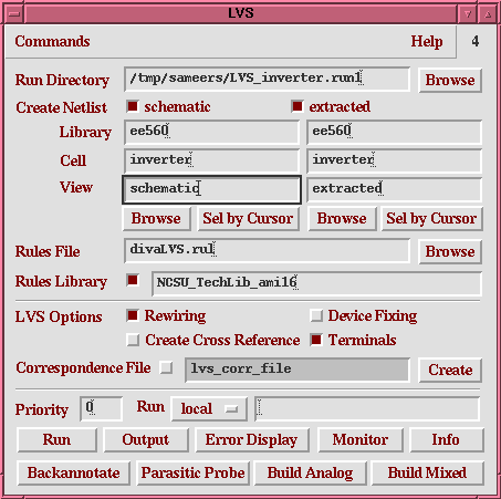
- Click on the Run button and wait !!
5. A pop up menu will appear notifying you of the successful completion or failure of the LVS job.
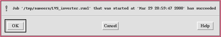
Click on the OK button.
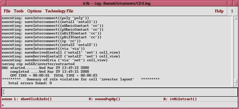
6. If you click on Job monitor window, you will see a window as shown
below. Click on the simulation button on the left.
(The following window
invocation of Cadence gives a insignificant error in the icfb window, which is
being looked into.. So don't worry about it for now !)
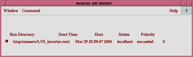
Then click on the Command → Show Run Log.
7. A window will pop-up and you will see the following. This is the si.log output file.
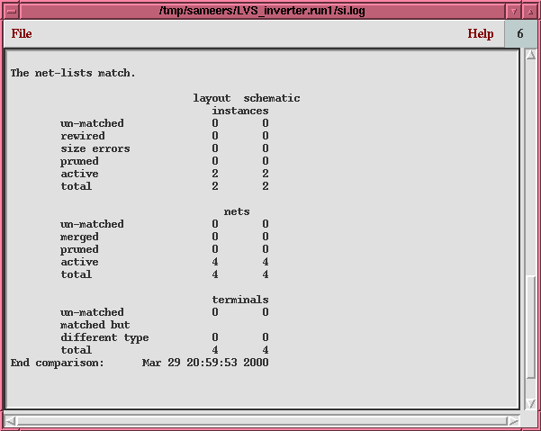
8. We see from the run log above that there are no errors in the comparison. However, there could have been error, if for example the W and L of the transistors in the schematic window didnot match with the W and the L of the transistors in the layout. If you have any errors, click on Error Display... in the LVS menu to view what went wrong. It is very beneficial if you click on Help in the si.log output window shown above. It will explain each of the terms in the above window in great detail.
The following points illustrate a situation if we had an error in the previous step.
9. By clicking on the Error Display, you would see the following.
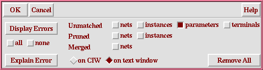
Select or deselect the various options so that the errors that will be shown are only those that you want to see at this point. In our case, the only errors we encounter is the size errors and to see that we select parameters under the Unmatched field.
10. Click on the Display Errors button. You'll see the errors being highlightedby a green dot in the extracted window.
11. To get more information about the error, click on the Explain Error button. Then move your cursor above the highlighted point/area (in this case the bright green dot) and click on the left mouse button. A pop up menu will appear. Sometimes the information given is not very helpful. This is where your problem solving skills come to play and are being sharpened.
12. Modify the layout or schematic appropriately and rerun the LVS till your design is perfectly matched.
13. There's also a feature which can help you in debugging especially checking the connection of your nets. You can access this feature by choosing Probe... from the Verify menu in your extracted view. A pop up window will appear as shown below. The following window may look a little different . It doesnot matter.
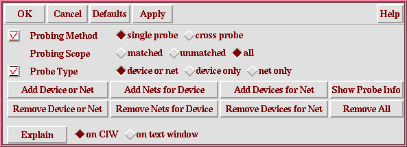
14. Click on the Add Device or Net button and then move your cursor to the net you want to be highlighted and click on the left mouse button. Anything that's connected to that net will be highlighted. An example of the highlight is shown below.