Create Schematics
At this point, you have created a library of your own and can begin the design process. For a full custom design, the process begins by creating a schematic, simulating it (whether in Verilog or HSpice) in order to optimize the performance, and then comes the layout (which is where you flaunt your artistic skills!). After the layout is completed, you need to extract the layout and compare it with the original schematic - a process called Layout Versus Schematic, in short LVS, verification. You will then perform a final simulation on the extracted layout which includes parasitic capacitances. The post layout simulation results is closer to reality and gives you a good idea of whether your design would work if fabricated. In this section we would be talking about creating your own Schematics.
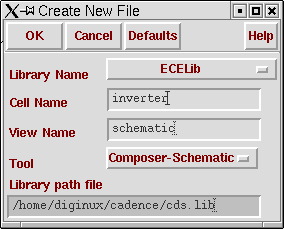
1. To create a schematic, click on File→New→Cellview in the CIW window. You could also click on the File→New→Cellview in the Library Manager Window to create a schematic. A pop-up menu will appear. Click on the library name button and select ee560. Then click on the Tool button to select Composer-Schematic. The View name will automatically change to schematic. Enter the name of the cell you wish to design in Cell Name. For the tutorial case, lets generate an inverter.
This will pop-up an empty Schematic Creation Window.
3. You need to bring devices into your design in this window. The following figure is what you are aiming for.
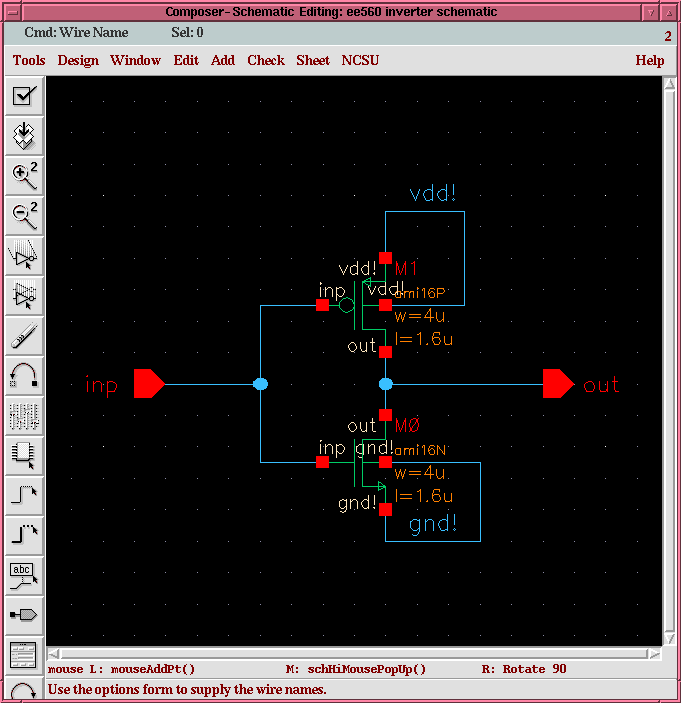
The following steps will teach you how to create a schematic like the one shown above.
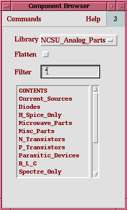
Click on Library and choose NCSU_Analog_Parts .Click on N_Transistors in the CONTENTS menu in the above window. Then choose nmos4 as your NMOS device. You can ignore the other pop-up menu which appeared alongwith the Component Browser window for now. To place the instance, click on the left mouse button.Another new instance will immediatedly become ready to be placed. If you need an additional nmos, you can reclick the left button in your schematic window. Press ESC to stop adding anymore nmos devices. (Note : ESC is the key to your escape from Cadence's persuasive nature. If you don't want Cadence to do what it is doing right now, you can always press the ESC key. Most of the times, cadence will yield to your requests)
3. To set the properties of the instance that you just placed, e.g. the width and length of the NMOS device, move your cursor on top of the device and type q. An object properties editing form will pop up.
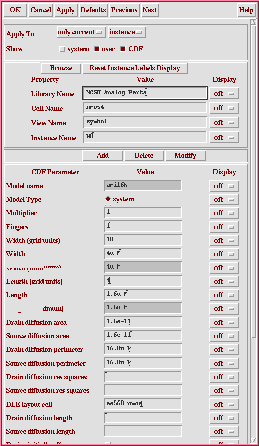
Fill in the value for the Length property by deleting whatever there is in that entry ,and then entering the proper length using the scientific notation of u as shorthand for microns, in this case it would be 1.6u. As soon as you enter the properties, an M will appear automatically and it will look like 1.6u M. Follow the same procedure for the Width property. You can also enter other properties in an analogous fashion, if desired, otherwise the default values will be used.
4. Repeat steps 2 and 3, but this time choose the cell pmos4 also in the NCSU_Analog_Parts library.
5. To place a wire to connect the two devices as depicted in the inverter schematic above (the blue lines), move your cursor to the point where you want the wire to begin. Then type w and move your cursor. You will see a yellow line connecting the starting point and the cursor. Click the left mouse button at the point where you want to change the direction of the wire. Wire the PMOS and NMOS devices as shown in the inverter schematic above.
6. The next step is to specify the input and output pins (the red colored polygon). With your cursor in the schematic window, type p and a pop up menu will appear.
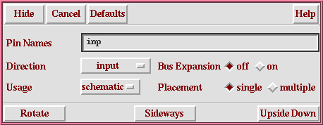
We will specify the input pin first. In the Pin Names field, type inp. The Direction is input and the Usage is schematic. Then move your cursor into the schematic window and you'll see the pin in yellow outline. Click on the left mouse button to place the pin. We'll now specify the output pin. Move your cursor back into the pop up menu and type out in the Pin Names field. This time, however, the Direction is output. Again place the pin at the desired location.
7. For every cell, you need to have supply pins or labels. For example you may need Vdd and Ground. You may have additional pins like the ones we had for inp and out, for the supply (vdd and gnd). Since most of your other cells (eg Nand gate, Nor gate) would be using the same supply Vdd and gnd, it is sometimes convenient to have them declared globally, so that you don't need to have a separate pin for the supply terminals within each cell. A global declaration can be achieved by labeling the net for the supply or ground or whatever is truly global in the circuit by a <labelname> followed by " ! " sign. The figure above for the inverter shows that vdd! and gnd! are two global nets.
Labeling can be achieved by typing the letter 'l' anywhere in the schematic window. This will pop up a
menu like the one shown below. Type in vdd! in the
Names field. Then click on Hide. Then once you
bring the mouse in the schematic window, you can just
move (not drag) your mouse till you locate it on the top of
the wire ( also called a net), plan to label. Then click on left mouse button.
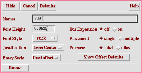
You label the net for the ground accordingly, by typing gnd! in the Names field.
Note:Labeling is not used just for global
declarations. It can also be used to label any wire with the name of your
choice. All nets with the same name are automatically
connected (
without drawing a wire). This is convenient, when your schematic design is huge
and drawing wires may make your circuit look messier. But you need to remember
that you should not end your labelname with a ! sign,
unless it is a global net.
8. Congratulations! You have just completed your first schematic in Cadence. To check and save your design, click on the first icon to the left of the schematic (it is the icon with a box and a check mark). You will be warned if you have any floating wires or pins. You can also perform the same function by selecting Check and Save from the Design menu of the schematic window. To close the schematic window, select Close from the Window menu in the schematic window.
QUICK USAGE REFERENCE:
1. Press 'p' to add pins
2. Press 'q' on the device/instance to edit properties for the
device
3. Press 'w' to add
wires
4. Press 'f' to fit the
schematic in
your schematic window.
5. Press 'l' to
label a wire.
6. Press 'Up' and 'Down'
arrows to move up and down within a schematic window.
7. Press 'ESC' to terminate any of the operations in the
schematic
window.